- HJTPV.com
- HJT Technology
- HJT Producers
- HJT Solar Panels
- HJT Solar Panel Mysolar Gold 740W
- HJT Solar Panel Mysolar Gold 640W
- HJT Solar Panel AEsolar COMET 720W
- HJT Solar Panel AESOLAR COMET 650W
- HJT Solar Panel Bi Chaser Akcome 120 Cells
- HJT Solar Panel HuaSun HS-B120DS
- HJT Solar Panel Jinergy JNHM120 Cells
- HJT Solar Panel Risen Hyper-ion
- HJT Solar Panel QW Solar Giwa5 730W
- HJT Solar Panel QW Solar Giwa5 640W
- HJT Solar Panel Risen RSM120
- Cleaning Robot
- HJT Solar CELLS
- News&Knowledge
- Contact
HJT Solar Review
HJT Technology
On this Site You Will Read About
Explore the Experts
WHAT IS HJT TECHNOLOGY?
Heterojunction (HJT) means that solar cell is not made with homogenous material like monocrystal cell. HJT is a combination of Moncristal Silicon and amorphous Silicon Thin-film/ Layer. This innovative Idea to combine to kind of Silicon was developed by SANYO with the name “HIT” (Heterojunction with Intrinsic Thin-layer technology). HJT technology combines the best advantage of crystalline silicon N-Type and thin-film giving:
- cell efficiency >25% and solar panel >22,8%
- the lowest temperature coefficient -0,24%
- very low annual degradation rate 0,25%
- NO LID&PID effects
- the highest bifacial 95%
Heterojunction (HJT) technology is an advanced solar cell design that merges crystalline silicon (c-Si) wafers with ultra-thin amorphous silicon (a-Si) layers, achieving high performance and efficiency.
Key Characteristics and Performance:
- Efficiency: HJT cells reach 22-24% efficiency, outperforming many traditional cells like PERC, which typically have around 20-22% efficiency.
- Temperature Coefficient: Around -0.24%/°C, meaning lower power loss as temperatures rise compared to conventional cells (typically around -0.35%/°C).
- Degradation Rates: Annual degradation is about 0.3-0.5%, significantly lower than traditional cells that degrade at 0.5-0.7% per year.
Advantages:
- Low Light-Induced Degradation (LID) and Potential-Induced Degradation (PID): LID and PID are reduced by over 90%, maintaining higher initial and long-term performance.
- Bifacial Gains: HJT cells are often bifacial, capturing light from both sides, with rear-side contributions adding up to 10-20% extra energy yield.
Manufacturing and Cost:
- Lower Silver Usage: 0BB (Zero Busbar) and Smart Wire Technology reduce silver costs by 50-70%, contributing to cost optimization.
- Production Costs: Higher than conventional cells, but with advancements, costs are lowering to improve competitiveness.
HJT technology offers high efficiency, low degradation, and strong temperature performance, leading to higher energy yields and long-term reliability, making it a standout choice for premium solar applications.
Explore the Experts
HJT TECHNOLOGY - history of development.
The story of Heterojunction (HJT) technology in solar photovoltaics is one of innovation and evolution, focusing on enhancing efficiency, performance, and durability. Below is a brief history of its development:
Early Development in the 1980s
- Origin at Sanyo: The roots of HJT technology can be traced back to the 1980s when Sanyo, a Japanese electronics manufacturer (later acquired by Panasonic), developed the “Heterojunction with Intrinsic Thin Layer” (HIT) cell. The idea was to combine the benefits of both crystalline and amorphous silicon to create a solar cell with high efficiency and excellent surface passivation.
Commercialization and Growth in the 1990s-2000s
- First Commercial HIT Cells: By the 1990s, Sanyo had commercialized the HIT technology. The key innovation was to use a crystalline silicon (c-Si) wafer as the core for high conductivity and two thin layers of amorphous silicon (a-Si) on either side for better surface passivation, reducing electron recombination and enhancing efficiency.
- Higher Efficiency and Temperature Performance: Throughout the 2000s, HIT cells became known for their high conversion efficiencies, low temperature coefficient (superior performance in heat), and low degradation rates compared to conventional cells.
Acquisition by Panasonic and Further Innovations (2010s)
- Panasonic’s Improvements: When Panasonic acquired Sanyo in 2010, it further refined the HJT process. By focusing on manufacturing efficiency and cell design, Panasonic was able to produce cells that reached world-record efficiencies (up to 24% in the lab and around 22-23% in commercial production).
- Improvement in Manufacturing Process: During this period, developments in transparent conductive oxides (TCOs) and improvements in laser and deposition techniques contributed to more efficient HJT production and a reduction in costs.
Industry-Wide Adoption and Technological Advances (2015-present)
- Broader Market Adoption: By the mid-2010s, other companies began investing in HJT technology, recognizing its potential for high efficiency and long-term stability. Manufacturers in China, Europe, and the U.S. started incorporating HJT technology into their product lines, seeing it as a natural successor to PERC (Passivated Emitter Rear Cell) and other existing technologies.
- Zero Busbar (0BB) Integration and Bifacial Modules: Innovations like Zero Busbar (0BB) technology (where busbars are eliminated to improve light absorption and efficiency) and bifacial modules (which can capture light from both the front and back) were adopted to maximize the energy yield of HJT cells.
Current Status and Future Outlook
- Increasing Efficiency and Reducing Costs: Today, HJT modules are among the highest efficiency commercial PV products, with typical efficiencies of 22-24%. The cost of manufacturing has continued to decrease due to advances in materials and production techniques, such as Smart Wire Technology (SWCT), which replaces traditional busbars with fine wires to enhance current collection and performance.
- Competition with Other High-Efficiency Technologies: HJT competes with other high-efficiency technologies like TopCon (Tunnel Oxide Passivated Contact) and perovskite-based tandem cells. However, HJT remains a favorite for its high performance, particularly in bifacial designs and its lower degradation rates over time.
Explore the Experts
HJT TECHNOLOGY vs TopCon.
Comparison between Heterojunction (HJT) and Tunnel Oxide Passivated Contact (TopCon) solar technologies, highlighting their advantages and current competition in the PV market:
Efficiency
- HJT: Achieves around 22-24% efficiency in commercial cells, with lab efficiencies reaching 26%.
- TopCon: Efficiencies are close to HJT, around 22-23.5% in commercial products, and have reached similar lab efficiencies of 25% or slightly higher.
Temperature Coefficient
- HJT: Around -0.22%/°C -0.26%/°C, providing better performance in hot climates.
- TopCon: Typically has a temperature coefficient of around -0.28%/°C–0.35%/°C, which is better than conventional cells but slightly less favorable than HJT.
Degradation
- HJT: Annual degradation rates are approximately 0.25-0.5%, with very low Light-Induced Degradation (LID) and Potential-Induced Degradation (PID).
- TopCon: Also has low degradation rates, around 0.35-0.6% annually, with improvements in LID and PID similar to HJT.
Bifacial Gains
- HJT: Offers bifacial designs with rear-side energy yield contributing an additional 10-20% to total power output.
- TopCon: Also available in bifacial designs, with rear-side contributions of around 10-15%.
Manufacturing Complexity and Costs
- HJT: Has a more complex manufacturing process requiring transparent conductive oxides (TCO) and low-temperature processing, resulting in higher initial production costs. However, advancements like Zero Busbar (0BB) and Smart Wire Technology are reducing costs, and silver paste usage is cut by around 50-70%.
- TopCon: Built on PERC architecture, TopCon cells require less drastic changes in manufacturing lines, making the transition less costly. The process involves tunneling oxide and polysilicon layers that are more compatible with existing PERC production lines, leading to a more cost-effective upgrade.
Market Position and Growth
- HJT: Known for high efficiency and low temperature losses, it’s favored for applications requiring premium performance. HJT has a growing market share, particularly in Europe and China, and continues to be adopted for utility-scale and rooftop installations due to its long-term reliability.
- TopCon: Due to its easier manufacturing transition and competitive efficiency, TopCon has been growing rapidly as an upgrade to PERC lines. Its lower production costs and close performance to HJT make it a strong contender, often preferred for cost-sensitive installations.
War of Domination in PV Market
- Current Market Share: PERC still dominates, but HJT and TopCon are both competing for the high-efficiency segment of the PV market. TopCon is gaining traction because of its easier integration with existing PERC lines, while HJT is seen as the next step for maximizing efficiency and long-term performance.
- Efficiency vs. Cost Trade-Off: HJT leads slightly in efficiency and performance, particularly in hot climates, while TopCon offers cost-effective production and comparable efficiencies. Both technologies are expected to erode PERC’s market share significantly over the next decade, with HJT pushing the boundaries of efficiency and TopCon focusing on cost-effective improvements.
In summary, HJT and TopCon are closely matched in terms of efficiency, with HJT having a slight edge in performance metrics but TopCon being more cost-effective to produce. The “war of domination” in the PV market will hinge on cost reductions, manufacturing advancements, and the ability to scale production while maintaining high efficiencies.
Explore the Experts
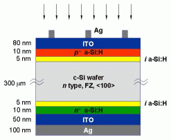
HJT cell structure
The manufacturing process of a Heterojunction (HJT) cell involves several key steps, combining the advantages of crystalline silicon (c-Si) with amorphous silicon (a-Si) layers to create a high-efficiency, low-degradation solar cell. Below is a step-by-step overview of how an HJT cell is made:
1. Preparation of the Crystalline Silicon Wafer
- Base Wafer: A thin N-type crystalline silicon (c-Si) wafer is used as the base. N-type wafers are preferred over P-type because they exhibit lower degradation and better performance over time.
- Cleaning and Texturing: The wafer undergoes a thorough cleaning to remove any surface contamination. Texturing is then applied to the surface to create a rough pattern, reducing reflections and improving light absorption.
2. Deposition of Intrinsic Amorphous Silicon Layers (a-Si)
- Intrinsic (i) Layer Deposition: Thin layers of intrinsic amorphous silicon (a-Si) are deposited on both sides of the wafer. This is done using Plasma Enhanced Chemical Vapor Deposition (PECVD) at low temperatures (below 200°C).
- Surface Passivation: These intrinsic a-Si layers passivate the c-Si wafer, reducing electron recombination losses at the surface and improving the cell’s efficiency.
3. Deposition of Doped Amorphous Silicon Layers
- Doping Process: On top of the intrinsic layers, doped amorphous silicon layers are added. On the front side, a p-type doped a-Si layer is deposited to form the emitter, while on the back side, an n-type doped a-Si layer forms the back surface field (BSF).
- Purpose of Doped Layers: These doped layers enhance the junction properties, enabling efficient separation and transport of charge carriers (electrons and holes), which are generated when the cell is exposed to sunlight.
4. Application of Transparent Conductive Oxides (TCO)
- TCO Deposition: Transparent conductive oxide (TCO) layers, such as Indium Tin Oxide (ITO) or Zinc Oxide (ZnO), are deposited on both sides of the cell using sputtering or chemical vapor deposition (CVD).
- Functions of TCO: The TCO layers serve two purposes: they act as anti-reflection coatings to improve light absorption, and they provide electrical conductivity to help collect and transfer the generated current from the cell to the external circuitry.
5. Grid and Contact Application (Interconnections)
- Front and Rear Contacts: To collect the current, fine metal gridlines (fingers) are printed on both the front and back sides of the cell. This can be done using screen printing or advanced techniques like Smart Wire Technology (SWCT).
- Zero Busbar (0BB) or Reduced Busbar Designs: Some HJT cells utilize Zero Busbar (0BB) technology or multiple thin busbars to reduce shading and enhance efficiency. These interconnection methods reduce the loss of active cell area and improve electrical performance.
6. Cell Annealing and Curing
- Thermal Processing: The cell is annealed at low temperatures (typically around 200°C), which helps in curing the layers and improving their electrical properties without damaging the silicon structure. HJT cells are processed at lower temperatures than traditional silicon cells, preventing wafer damage and enhancing cell performance.
7. Testing and Sorting
- Electroluminescence and IV Testing: The cells are tested for their performance characteristics, such as efficiency, voltage, and current. Electroluminescence testing is used to detect defects and ensure uniformity in production.
- Sorting and Grading: Based on the test results, the cells are sorted into different performance grades to ensure modules have consistent power output.
Summary of HJT Cell Structure
The final HJT cell consists of:
- A crystalline silicon (c-Si) wafer core that acts as the main active layer.
- Thin intrinsic and doped amorphous silicon (a-Si) layers on both sides, providing surface passivation and forming a heterojunction.
- Transparent conductive oxide (TCO) layers for improved light capture and electrical conductivity.
- Fine metal gridlines or wires to collect and transport the generated electrical current.
By combining these materials and structures, HJT cells achieve high efficiency, low degradation, and excellent performance under varying temperature and light conditions. The process leverages both the high conductivity of crystalline silicon and the superior passivation and light absorption capabilities of amorphous silicon.
Explore the Experts
HJT 740W CLub
The “740W+ Club” refers to a segment of high-power HJT (Heterojunction with Intrinsic Thin-layer) solar modules that aim to deliver power outputs exceeding 740W per panel. This club symbolizes a significant step forward in PV module efficiency and power output, driven by the rapid advancement of HJT technology and related innovations. Here’s a detailed breakdown of what this club entails and its significance:
1. High-Efficiency BOM Configuration
- The 740W+ power output is achieved by utilizing advanced BOM (Bill of Materials) configurations that combine high-quality materials and processes. Key components contributing to the higher wattage include:
- High-Purity Silicon Wafers: The use of larger and higher-quality silicon wafers, typically 210mm in diameter or half-cut configurations, reduces resistive losses and enhances efficiency.
- Ultra-thin Wafer Technology: Reducing the thickness of wafers to around 100 µm, with potential further reductions, allows more efficient use of silicon without compromising performance.
- High-Efficiency Cell Structures: Optimizations such as reducing surface recombination and implementing highly effective passivation layers are crucial in achieving such high outputs.
2. Advanced Technological Features for Power Boost
- Full-Open-Mesh Metallization (FOG Technology): This technology allows for the printing of fine and efficient gridlines that minimize shading and increase light absorption, thereby improving power output.
- 0BB (Zero Busbar) Design: The use of zero busbar technology allows for uninterrupted current flow across the cell surface, improving overall efficiency and contributing to a power boost of around 5W compared to traditional designs.
- Innovative Light-Trapping Techniques: Enhancements such as back-side texturing, passivated contact layers, and bifacial designs (double-sided light absorption) ensure maximum light capture and conversion into electricity.
3. Bifaciality and Higher Power Yield
- Bifacial Design Benefits: The 740W+ HJT modules often employ bifacial technology, where the rear side of the panel also absorbs light reflected from the ground, increasing the energy yield by up to 15-30% depending on installation conditions.
- Lower Temperature Coefficients: HJT cells have lower temperature coefficients (typically around -0.24%/°C) than many other cell technologies, ensuring better performance under higher temperature conditions and enhancing the module’s power output.
4. Optimized Manufacturing and Cost-Efficiency
- Reduced Use of Silver (Ag) in Metallization: Innovations in electrode pastes, such as using silver-coated copper (AgCu) or silver-clad aluminum, have significantly reduced silver content by around 30-50%, helping to lower material costs while maintaining high performance.
- Streamlined Production Process: HJT modules are manufactured using advanced, automated lines that increase production speeds and ensure uniform quality. This results in efficient mass production and contributes to the lower costs per watt.
5. Market and Application
- Utility-Scale Solar Farms: The 740W+ HJT modules are primarily aimed at utility-scale projects, where high-power output per panel reduces balance-of-system (BOS) costs and optimizes space utilization.
- Compatibility with Modern PV Systems: Due to their high efficiency and power ratings, 740W+ HJT modules are highly compatible with modern inverter technologies and mounting systems, enabling optimal energy yields.
6. Projection and Industry Impact
- Power Efficiency Trends: The 740W+ Club sets a benchmark for the solar industry, as advancements in HJT are expected to push efficiencies and power outputs even higher in the coming years, with targets reaching 28-29% efficiency and potentially surpassing 800W per module.
- Competitive Advantage over PERC and TOPCon: The “740W+ Club” modules offer a significant competitive advantage over other technologies like PERC (Passivated Emitter and Rear Cell) and TOPCon (Tunnel Oxide Passivated Contact) due to their higher efficiencies, bifacial gains, and overall power output. This makes them more attractive for developers aiming to maximize energy yield and reduce system costs.
Summary
The 740W+ Club represents a new standard in solar module performance, characterized by high efficiency, advanced material usage, and innovative design features that collectively boost power output. These modules are becoming increasingly attractive for large-scale solar farms and projects aiming for maximum energy production, offering significant advantages in terms of energy yield, cost per watt, and space efficiency. The ongoing developments in HJT technology suggest that the benchmarks set by the 740W+ Club will continue to rise, pushing the boundaries of solar power capabilities.
Why HJT solar panels?
Best Performance
Highest Efficiency and power of solar panels 710W
Long Warranty
30 years with only 0,25% annual degradation
inspiring technology
N-type & Bifacial Cells cover in Glass glass frame
What HJT Technology offer
HJT Advantage

state-of-the-art Solar Solution
How is construct HJT CELL?
Differences Between HJT and PERC
Differences between HJT and N-Type and PERC Unlike standard (PERC and N Type) crystalline solar cells which are homogeneous devices. Which means that the p-type and n-type semiconductor layers are formed on the same base material. Heterojoint cells, on the other hand, are made by combining two different types of materials. In the case of HJT silicon, the connection is made between the crystalline and amorphous silicon materials.
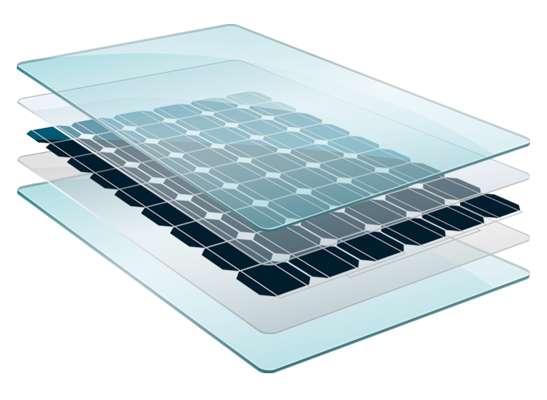
HJT Solar Panel Constrution
Sanyo, which is a pioneer of HJT technology. He proposed placing an internal amorphous layer between the enriched surfaces of amorphous and crystalline silicon. This gave rise to the famous and patented "Heterojunction Sanyo" with an "Intrinsic Thin" layer, commonly known as HIT. For practical reasons HIT structure composed of crystalline silicon wafer, typically n-type, disposed between the inner and opposite enriched layers of amorphous silicon deposited at both sides and a transparent conductive oxide (TCO) on top. Almost all existing HJT concepts are based on this template
N-Type HJT Solar Modules
In some ways, solar cells are really simple. The light shines into them, precipitating electrons from silicon atoms. A cell is built in such a way that electrons are often blocked from returning to the atoms they came from. Instead, they travel through the fine mesh of wires at the top of the cell to the back of the cell and are transformed into electricity as they travel. This is what is done in the P-type solar cell because P is positive (positive) and the solar cell has a positive base that attracts him negatively charged electrons. The exact opposite process takes place in N-type cells. Since the base is negative, the electrons travel from the negative bottom to the positive top.
Best HJT Producers with Best Direct Prices
go beyond your PV limits
Why HJT Panels Are The Best?
Best Advantage of Hjt Solar Panels

Explore the Experts
Best HJT Producers
commit to HJT Solar Revolution
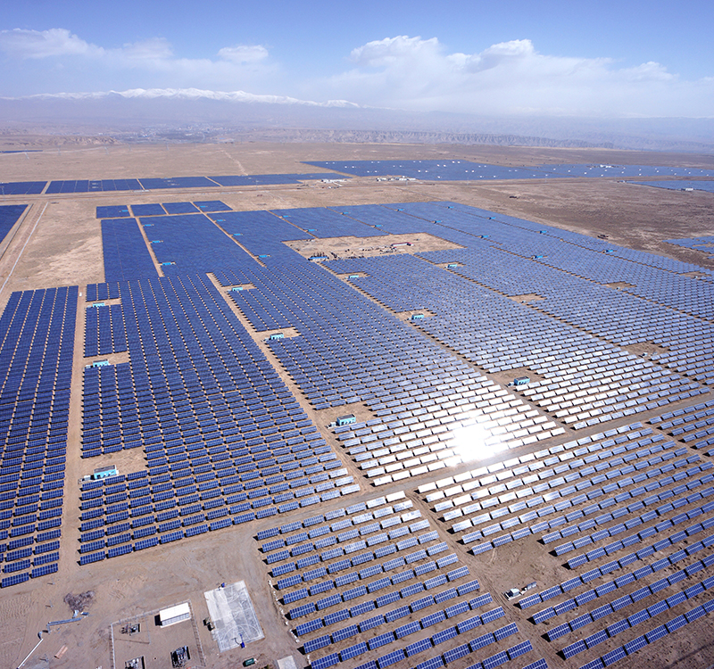
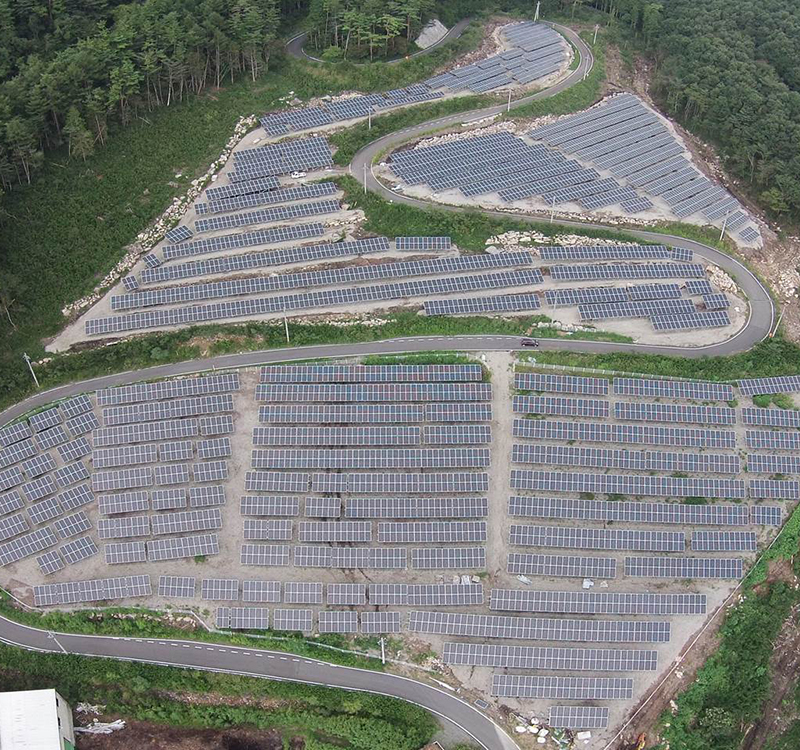
HJT Solar Panel is best Solution for Utility scale investitions
Up 15% more production in 30 years
UP to 9,3% less construction costs
6,4% lower cost of MC4 and cables
Up to 10.4% lower labor costs
LCOE reduction 4,4%
Up to 20% lower BOS costs
All You Need To Know About HJT Technology
frequently asked questions
HJT efficiency can achieve even 27%. But usually producers like Acome and Jinergy use Heterojunction solar cells with 24%-25% efficiency. Compare to PERC Cell, HJT can achieve even 20% more power.
HJT solar panels have the best efficiency in serial production. Scope of it is between 21%-22,5% with R&D plan even to 26%. HJT module has the best performance and most reliable characteristic resistance for most common fail from all over solar technology.
HJT solar Panels with 120 cells have a scope of power between 370W-390W and for 144 cells 425W – 470W. At the end of 2021 Power of HJT modules will achieve >500W and in soon future will be >600W.
HJT technology ensures a long safe warranty for 30 years of production and 12 -30 years for a panel, depends on the producers. It’s more approx. 5 years than common PERC panels.
HJT solar panels are value for money solutions. Compare with standard backsheet modules, the price for Heterojunction is a little bit more. But compared with Bifacial, glass-glass solar panels, HJT is the best solution and has more advantages worth a few % higher price.
Higher power, bifaciality, efficient production under extreme conditions, combined with the world’s lowest degradation, no LID and PID effects and a double glass structure (GLASS-GLASS), allows you to generate significant savings over 30 years of use compared to PERC panels.
Glass is the best protection for the silicon cells that are the heart of the photovoltaic module. A cell is a unit that generates electricity, but it is made of a delicate material that needs to be reinforced and secured externally. For this purpose, we have a good ally in the form of solar glass, which, in addition to being transparent, is an electrical insulator.
HJT PV team is not only a trusted advisor but solar panels broker. We are helping Clients from all over the world connect to trusted and checked HJT producers. Direct cooperation ensures the best prices and fast delivery, to all destinations.
HJT Sales and distribution
EPC Cooperation
general contractor of photovoltaic investments
Distributor In Europe
Container and Mega Watt sales
Photovoltaic Broker
mediation in the purchase directly from the manufacturer

